
삼성, 450단 NAND 칩 2개를 900단 V-NAND에 쌓다
페이지 정보
작성자 playbbs 작성일 26-05-31 15:24 조회 15 댓글 0본문
[AI 하드웨어 번역 뉴스]
삼성, 450단 NAND 칩 2개를 900단 V-NAND에 쌓다
[핵심 요약 및 번역]
삼성전자는 1000단 낸드플래시 저장모듈 생산 목표를 향해 꾸준히 노력하고 있다. 그러나 제조 복잡성이 증가함에 따라 단일 칩으로는 이를 달성할 수 없습니다. 대신 450단 V-NAND 모듈 2개를 900단 V-NAND 칩 1개에 적층하는 고급 패키징 솔루션으로 전환하고 있습니다. 이번 제조 성과를 처음 보도한 ET뉴스에 따르면, 삼성전자는 하이브리드 본딩을 통해 구현되는 웨이퍼 스태킹의 변형인 CMB(Cell Multi-Bonding) 기술을 사용하고 있다. 이 프로세스는 융합되어 단일 칩을 생성하는 내장 금속 범프를 사용하여 두 개의 실리콘 칩 사이에 영구적인 결합을 형성합니다. 여러 개의 다이 또는 삼성의 경우 여러 개의 전체 실리콘 웨이퍼를 두 개의 칩 백엔드를 함께 쌓아서 연결할 수 있습니다. 삼성의 자산...
[상세 정보 및 원문 이미지]
Samsung is steadily working towards its goal of creating 1000-layer NAND Flash storage modules. However, as manufacturing complexities increase, the company cannot achieve this with a single chip. Instead, it is turning to advanced packaging solutions to stack two 450-layer V-NAND modules into a single 900-layer V-NAND chip. According to ET News, which first reported this manufacturing achievement, Samsung is using Cell Multi-Bonding (CMB) technology, a variant of wafer stacking achieved through hybrid bonding. This process forms a permanent bond between two silicon chips using embedded metal bumps that are fused together to create a single chip. Multiple dies, or in Samsung's case, multiple whole silicon wafers, can be connected by stacking two chip back ends together. Samsung's proprietary process, called CMB, paves the way for 1000-layer V-NAND chips by 2030.
Early last year, Samsung unveiled its 10th-generation V-NAND technology, enabling over 400 layers on a single module. The company also introduced hybrid bonding for the first time, indicating that the technology has since been refined. Interestingly, wafer bonding on already thick 450-layer designs is challenging due to wafer warping. Thankfully, Samsung developed microscopic chucks to address this, along with new bonding techniques to correct overlay issues and misalignment errors when wafers are bonded together. Within the NAND itself, Samsung created new bitline and wordline structures to help manage power consumption and maintain reasonable individual chip sizes.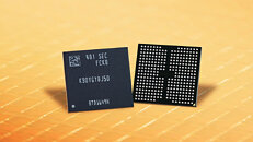
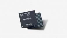
Early last year, Samsung unveiled its 10th-generation V-NAND technology, enabling over 400 layers on a single module. The company also introduced hybrid bonding for the first time, indicating that the technology has since been refined. Interestingly, wafer bonding on already thick 450-layer designs is challenging due to wafer warping. Thankfully, Samsung developed microscopic chucks to address this, along with new bonding techniques to correct overlay issues and misalignment errors when wafers are bonded together. Within the NAND itself, Samsung created new bitline and wordline structures to help manage power consumption and maintain reasonable individual chip sizes.


출처 원문: 소식 원문 보기
* 본 포스팅은 해외 IT 매체의 소식을 실시간 수집 및 번역하여 제공하는 인공지능 뉴스 로봇입니다.
관련링크
- 이전글 (PR) 공급 부족으로 인한 가격 인상으로 2026년 1분기 글로벌 NAND 플래시 상위 5개 공급사 합산 매출 전분기 대비 83.7% 증가
- 다음글 (홍보) Synology, 새로운 FlashStation FS200T 출시 발표
댓글목록 0
등록된 댓글이 없습니다.